Experiment 4 – AM Detector

Michael Smith
ELEC 3030-RF Systems Lab
Date of Lab - Friday, October 1, 2021, 1 p.m.
Experiment 4 – AM Detector
Today’s Date - October 11, 2021
Introduction
The AM detector’s job is to extract the audio signal, or envelope, from the AM signal. This audio signal is then amplified and passed to the speaker. In this lab I had to investigate a very simple diode detector followed by a biased diode detector for better performance. In the prelab, I became familiar with both using LTspice. Also, I breadboarded and experimented with a complementary feedback pair (CFP) detector circuit which has a clear advantage over the diode detector circuits. In this lab, we had to breadboard and test the simple diode detector, Figure 4.4, biased diode detector, Figure 4.6, and CFP detector circuits, Figure 4.10. After testing each of these circuits I choose to use the biased diode detector circuit in my radio’s audio amplifier.
In order to cut on redundancy and reduce the addition of unnecessary images, I have labeled my images the same as the images in the lab instructions. In other words, if the lab instructions say to recreate the circuit in Figure 4.4, I have labeled the circuit I recreated from the lab instructions, Figure 4.4. Likewise, if we are to recreate Table 4.3, I have labeled my Table 4.3 same with graphs. Since the person grading this paper is very familiar with the pre-lab and lab instructions, I don’t see the need to add the image that has to be recreated when the reader has that information in front of them. Also, I feel if you must compare lab instructions of Figure 4.3 to my Figure 4.3, it cuts down on confusion of numbering and labeling.
Part 4.5 Steps 1-6
A very simple detector circuit consists of a diode rectifier circuit, with an RC time constant chosen fast enough to follow the audio signal, but too slow to follow the carrier. This part of the experiment was to have us switch out resistor R1 with different values and notice the various discharge times. We then had to breadboard our circuit like Figure 4.4. We had to select a carrier frequency fc = 200kHz, internal modulation for intelligence frequency fi = 1 kHz and set our modulation to 50%.
For step #4, using my Digital Multimeter (DMM), my input is 0.05V and my output is 0.11V. I examined my output signal as the input signal was increased. The best result I achieved was when my input was 1.4Vpp with no input capacitor.
For step #5, I adjusted the signal amplitude so that I have an easy to read, steady input and output signal. I changed my R1 to 10kΩ. I observed the signal to be 0.06V.
For step #6, Keeping all the setting as I had before except in my circuit, I changed R1 to 100kΩ. I observed the signal to be 0.01V.
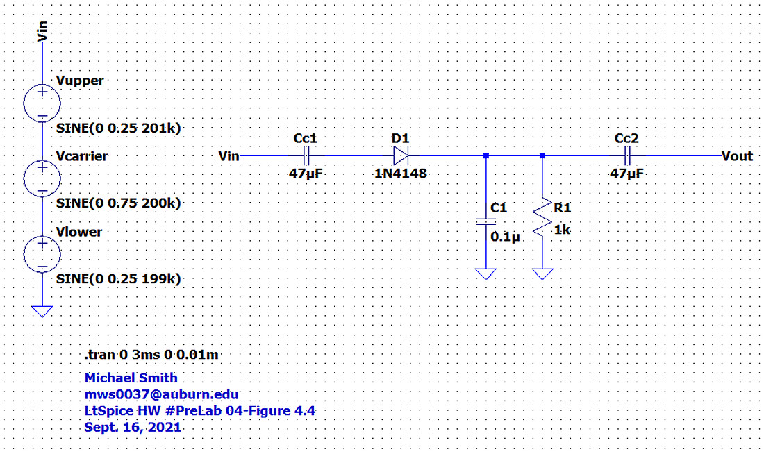
 Figure 4.4 – LTspice schematic of an AM detector.
Part 4.5 Step 7
In part 4.5 step #7 we are introduced to the Biased Diode detector because of the limitations of the simple diode detector. The simple detector circuit works fairly well (can extract audio signal from AM input) as long as the signal is strong enough to turn on the diode, it then tends to be too strong for the audio amplifier, so the output is distorted. But usually, the signal coming into the detector is rather weak, and the output suffers because the diode doesn’t turn on. A remedy of this is the bias diode detector. To see this for ourselves we then had to construct and test the circuit in Figure 4.6 from our lab instructions.
I fed a suitable AM signal to this detector circuit and examined the results using the dual channel feature of my Oscilloscope as before. I varied my AM signal levels from 50mV to 500mV. From these variations I realized the input voltage set at 200mV worked best. For sample waveform see Figure 1 below.
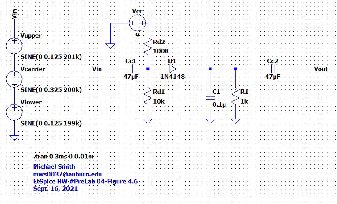 Figure 4.6- Biased Diode Detector Circuit
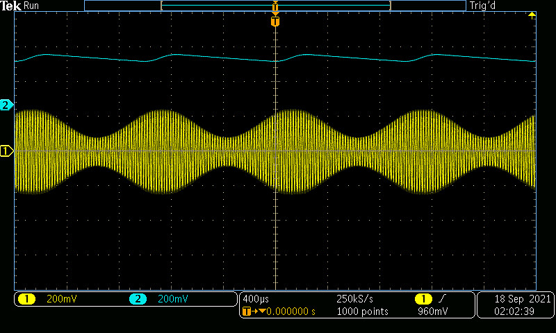
Figure 1 – Sample waveform of AM signal going through Biased Diode Detector
Part 4.5 Step 8
Next, we needed to construct the Complementary Feedback Pair (CFP) detector like what is shown in Figure 4.10. This is a modification of the Common Collector based AM detector, see Figure 4.8. The construction consists of adding a pnp transistor and a collector resistor to the npn of a Common Collector detector. When the input signal is high, both transistors are on and the Ce1 capacitor charges. When input signal is low, both transistors cut off and Ce1 again discharges through Re1. Rc1 is added so that more current flows through the pnp transistor and provides additional current for more rapidly charging Ce1. To see this for ourselves we then had to breadboard and test the circuit in Figure 4.10 from our lab instructions.
I fed a suitable AM signal to this detector circuit and examined the results using the dual channel feature of my Oscilloscope as before. I varied my AM signal level, from 50mV to 500 mV. From these variations I realized the input voltage set at 200mV worked best. For sample waveform see Figure 2 below.
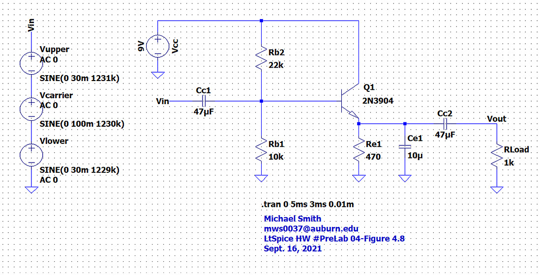 Figure 4.8a – A common-collector based AM detector at 30mV, 100mV, 30mV
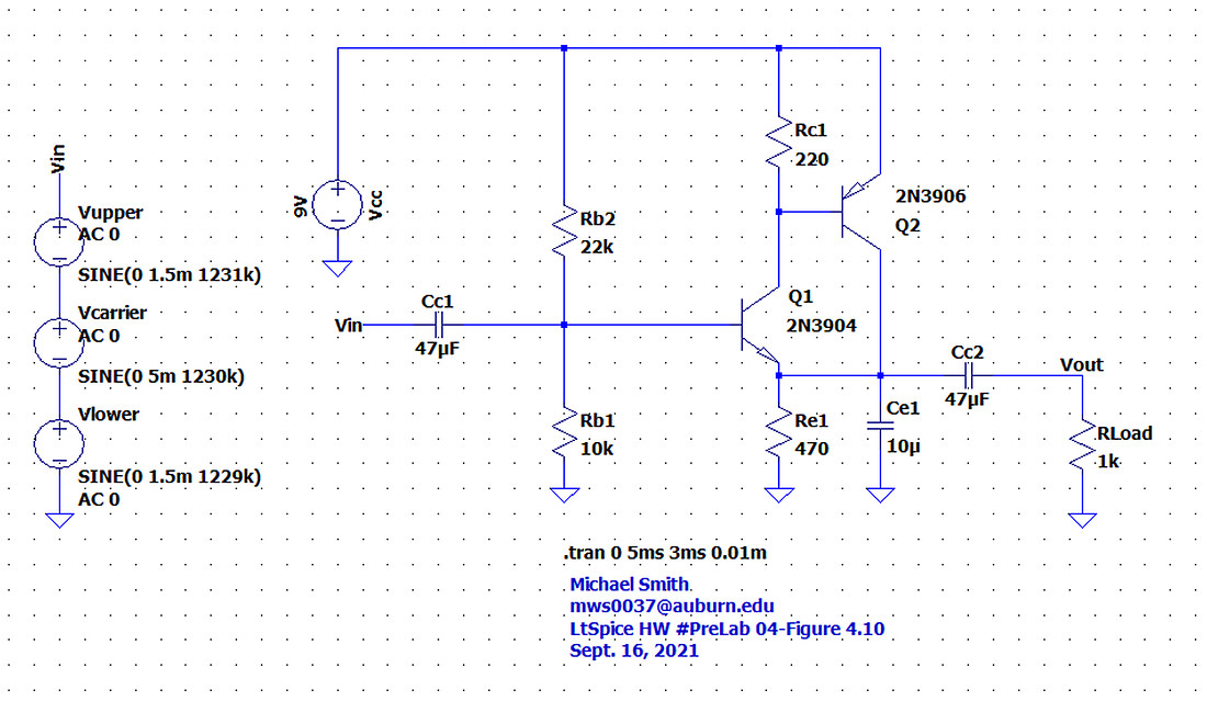 Figure 4.10 – Complementary Feedback Pair (CFP) Detector
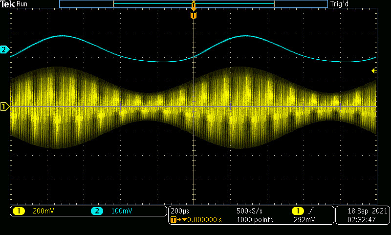
Figure 2 - Sample waveform of AM signal going through CFP Detector
Part 4.7 & 4.8
In the final part of our lab, we had to add our AM detector of choice to our radio. My first inclination was to use CFP detector. After I added it to my circuit in both simulations and physical construction, it did not perform as I expected. I then removed it and added a Biased Diode Detector to my AM radio similar to Figure 4.12. In both simulation and physical construction, it performed well. I replaced the Rload in my circuit with my speaker. I set my function generator to create an AM signal with the carrier signal set to 1230 kHz, my intelligence frequency was set to 1kHz with a 50% modulation. At a setting of 200mVpp the sound I received from my speaker was clear and nice.
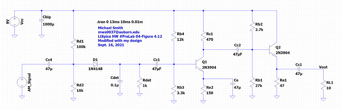
Figure 4.12 – Biased diode detector circuit added to the CE-CC version audio amplifier.
Conclusion
I am writing this report for Lab 4 after I have completed the Prelab and Lab for Lab 5. From looking at my plots from Lab 4 and Lab 5, my first inclination was to use a CFP detector. I constructed the circuit, and after running simulations and testing the constructed circuit, it was clear that it did not work as I expected. So, I decided to use the biased diode and common collector detector circuit. From the simulations and resulting graphs, and after I built and tested my circuit, this combination produces more desirable results for me.