Experiment 2 - Common-Emitter Amplifier

Michael Smith
ELEC 3030-RF Systems Lab
Date of Lab - Friday, August 27, 2021, 1 p.m.
Experiment 2 – Common Emitter Amplifier
Today’s Date - September 13, 2021
Introduction
The purpose of Lab 2 was to get us familiar with the Common-Emitter Amplifier (CE Amp) Circuit. Throughout the prelab we used LtSpice to change many parameters of a CE Amp to see how it changes the output, gain and many other aspects of the circuit. For more details on that, see my PreLab #02 report. For this lab we wanted to take aspects of what we learned through simulation and then construct the circuit on our breadboard. Through several LtSpice simulations and actual breadboarding we became familiar with the CE Amp circuit. Also, through changing different components in the circuit we became familiar with the gain and bandwidth. Also, these changes we made in our simulation were to help prepare us to physically breadboard a Common-Emitter Amplifier circuit.
Step 1
To begin with, we had to construct the DC circuit on our breadboard just like figure 2.8, from our lab instructions, see Figure 1. Then we had to use a Digital Multimeter (DMM) to measure the voltage readings of several different parts of our circuit, see Table 1. The point of this was to see if our transistor was operating in forward-active mode. You can see from Table 1 that my VBE = 0.718V, which means my circuit is in forward-active mode. You can see in Figure 2 the input and output signals from my circuit.
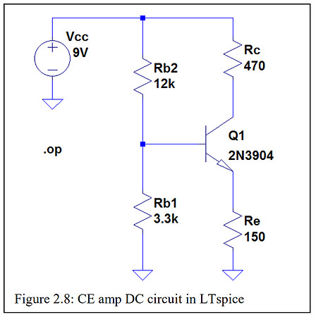

Figure 1- Figure 2.8 From Lab Instructions

Table 1 - Circuit Voltages
Step 2
The next step was to add the AC components to our circuit like Figure 2.11 from our lab instructions, see Figure 2. We had to use the dual mode of our oscilloscope to view the input and output signal of our oscilloscope at the same time, see Figure 3. Then we had to determine our voltage gain based on switching out our load resistor with resistors of various resistances. You can see from Table 2 and the resulting graph, Graph 1, as we increase our load resistance our gain increases. If we switched out one of the resistors with an 8Ω impedance speaker we could expect the CE amplifier to have a voltage gain close to 3V, because that is very similar to the gain of using a load resistor of 10Ω.
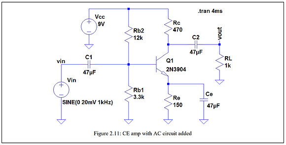
Figure 2 - Figure 2.11 From Lab Instructions
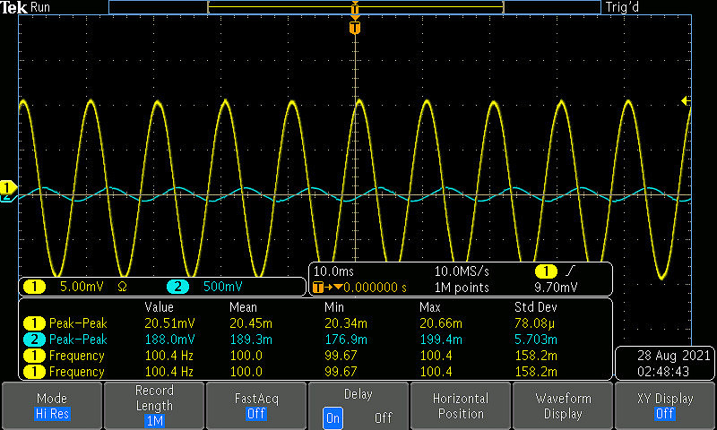
Figure 3 - 1kHz sine wave with 10mV amplitude
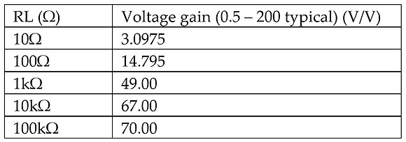
Table 2 - Gain compared with load resistance
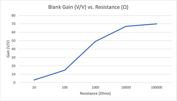
Graph 1- Blank Gain (V/V) vs. resistance (Ω) for plotting Table 2 data
Step 3
The challenge that was presented to us next was to change the load resistance with its default value of 1kΩ but measure the gain at different frequencies and create a Bode plot from the data. To get accurate information and receive a clear visual picture of changing frequencies we had to continuously change the time base on our oscilloscope. Additional fine adjustments were required with each step. You can see the resulting measured voltage gain in Table 3, along with the calculated gain in decibels. From that data you can see the resulting Bode plot in Graph 2. This information helped us calculate the half power bandwidth. The half-power bandwidth also called the 3dB bandwidth is the frequency range shown on a Bode plot over which the gain is within 3dB of the peak gain. From my plot the estimated 3dB bandwidth is 300 kHz.
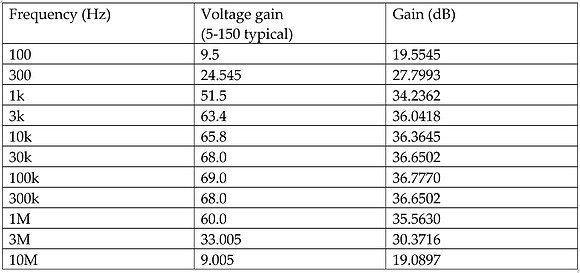
Table 3 – Bode Plot Data for CE Amp
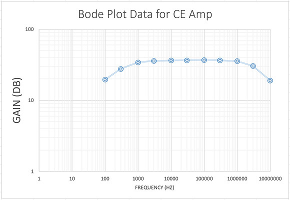
Graph 2- Blank Gain (V/V) vs. resistance (Ω) for plotting Table 2 data
Conclusion
The need to become familiar with the various amplifier circuits is extremely important. Various amplifiers are needed because of the countless different needs of engineers in many different situations. This lab focused on getting us familiar with how constructing the circuit in different ways changes the gain and bandwidth. Using the knowledge from our simulations and then constructing the circuits ourselves gave us invaluable knowledge and experience. This practice will help us in future circuit designs.